
-
真诚回报社会、客户、员工及股东
-
Provide customers with total solutions for grinding and polishing
-
Truth seeking , Innovation, Enhancement, Achievement
SOLUTION
Union Precision
Semiconductor packaging
In semiconductor packaging, a ceramic substrate is a special process plate in which copper foil is bonded to the surface of the ceramic substrate direcly (single or double-sided) at high temperature. The mainly types include Beryllium Oxide (BeO), Alumina (Al2O3) and Aluminum Nitride (AlN), Silicon Nitride (Si3N4).
characteristic:
1. Strong mechanical stress and stable shape;
2. Excellent thermal cycle performance, cycle times up to 550,000, high reliability;
3. Same with PCB board ((or IMS substrate)) can be etched out of a variety of graphic structure;
4. No pollution and pollution-free;
5. Wide temperature range -55℃~850℃;
6. Thermal expansion coefficient is close to silicon, simplifying the production process of power module.
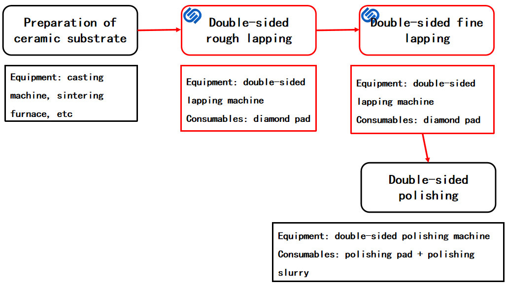
Processing process:
Ceramic substrate rough grinding process effect
| Diamond Pad Specifications | Rough grinding diamond pads for ceramics |
| Processing results | Processing data |
| Removal rate(um/min) | 10-15 |
| RoughnessRa(um) | <0.6 |
Ceramic substrate rough grinding process effect
| Diamond Pad Specifications | Rough grinding diamond pads for ceramics |
| Processing results | Processing data |
| Removal rate(um/min) | 7-10 |
| RoughnessRa(um) | <0.4 |
Interested in the products we offer?
We are happy to share our knowledge with you and are always happy to ask any further questions you may have.

Contact us
Technical support
Contact us
Contact us


Copyright © Henan Union Precision Material Co., Ltd., Powered by www.300.cn SEO
Contact us
Tel:+86-371-56589186 56589187
E-mail:market@union-diamond.com
Technical support
Contact us
Copyright © Henan Union Precision Materials Co., Ltd.,